| |
 Cheap
processor intelligence is being built into virtually every controller chip
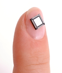
released today—chips which are no larger than a thumbnail! This runs the gamut
from sensors to communication chips to A/D and D/A chips to power chips to
microcontrollers. Yesterday’s 12" x 12" controller board, multi-card backplane
system, or three-card stack has been shrunk into single chip solutions with
USB, I2C, or SPI output! The result...appropriate board level form factors must
be re-thought. Cheap
processor intelligence is being built into virtually every controller chip
released today—chips which are no larger than a thumbnail! This runs the gamut
from sensors to communication chips to A/D and D/A chips to power chips to
microcontrollers. Yesterday’s 12" x 12" controller board, multi-card backplane
system, or three-card stack has been shrunk into single chip solutions with
USB, I2C, or SPI output! The result...appropriate board level form factors must
be re-thought.
Scaling down form factor footprint sounds easy enough, right? While smaller
semiconductors encourage smaller form factors for embedded applications, the
success of a form factor resides in having sufficient space for appropriately
defined connectors. Connectors have become, for lack of a better word, the
"bottle neck" to shrinking form factors. "Connectorology" is the key to
shrinking form factors appropriately for embedded OEM users.
The study of connectors and their mix of protocols, aptly coined
"connectorology," ensures OEMs maximize their efficiency and effectiveness. For
example, a "thumbnail" SOC chip offers several system level protocols users
might want to implement in their embedded application. To alleviate the burden
on the OEM, board level manufacturers are challenged with supplying a connector
to facilitate access to these protocols. Typically there are three approaches
to choosing a connector.
One way is to bring out each protocol supported by the CPU or SOC chip to
individual connectors. This approach typically works well for what is commonly
called a "reference design" board. The board size is defined by the number of
connectors required to communicate with all of the I/O options from the chip.
This board typically falls short of the needs of OEM users because the board is
maximized for the chip’s performance with little regard to the needs of an
embedded system. In this case, all types of I/O are equal and have an equal
position on the board which enlarges the physical dimensions of the boards not
to mention adds costs for multiple connectors (see Figure 1).

Figure 1
The second approach is for the board level manufacturer to randomly "stuff"
several protocols into a compact connector coming off the board with hopes that
it meets the user’s needs. While this approach is easy for the board level
manufacturer and appears at first glance to meet the need for smaller
footprints, it shifts a significant burden and cost to the user and adds bulk
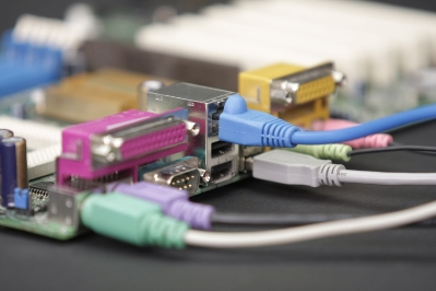
in unsuspected places. Users find they need to purchase a customized "breakout"
board to gain access to the protocols or signals from the connector. In the end
what was saved on an "inexpensive" single board computer is spent in custom
cabling and mounting hardware (see Figure 2) needed to access the I/O—a cost
easily overlooked in planning a system.

Figure 2
Embedded OEM users often find board-to-board communication the most cost
effective and efficient value for their system. The best approach to choosing a
board-to-board connector scheme is to evaluate the I/O and communication
protocols required by the system, plus the power, reliability and energy
demands, not to mention the overall assembly environment and budget for the end
product. A complete system approach emphasizes the value of selecting a
popular, industry-supported board-to-board stacking standard which clearly
defines the appropriate mix of protocols for the system. This ensures that the
user does not have more cost or complexity than he or she needs burdening one’s
system on multiple levels including form factor size. It also ensures that the
user does have what he or she needs and therefore doesn’t have to add
expensive, bulky cables or breakout boards. A well-defined connector specifying
pre-defined protocols enables OEM users to gain valuable access to common
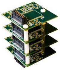
add-on I/O devices in the most efficient and effective space; the best example
of this is StackableUSB™ (see Figure 3).
 
Figure 3
|
| |
|
|